Areas of Plasma Application

04.

Semiconductor Packaging

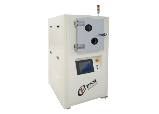
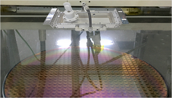
  • - AP plasma (M electrode) is applied to the FOWLP packaging / PLP molding pretreatment process
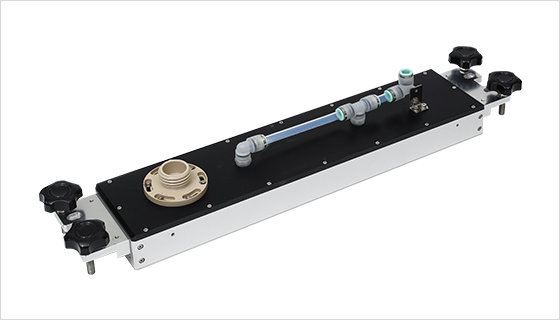
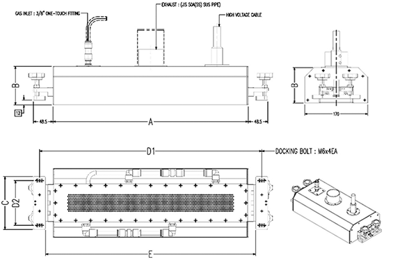
Semiconductor

APM Electrode

  1. 1. Applied to FO-WLP, PLP molding pretreatment process and BGA substrate final cleaning process
  2. 2. It is easy to operate and maintain.
  3. 3. ESD-free & outgassing-free

Specification

Semiconductor

Unit : mm

* D1 x D2 – Docking point (M6 bolt x 4ea)
200M 300M 300M
A 282.4 382.4 482.4
B 95 95 95
C 130 130 130
D1* 384.4 448.4 548.4
D2* 110 110 110
E 318.4 418.4 518.4
Plasma
Area
210 310 410
Weight 5Kg 6Kg 7Kg
Brochure Movement
  • - DF vacuum plasma is applied to the underfill pretreatment process to improve reliability

DF Vacuum Plasma System

  1. 1. Hydrophilic surface treatment process before FC BGA underfill
  2. 2. The PSM's unique vacuum system and uniform gas supply technology enable stable equipment operation
  3. 3. It is easy to operate and maintain.